Interested in graphene deposition at high speeds, and using a broader range of substrates at reduced temperatures - read on!
Interested in graphene deposition at high speeds, and using a broader range of substrates at reduced temperatures - read on!
Published on 29 Jul 09:01 (almost 2 years ago) by AquaTTDiscover the innovative PECVD processes and other competencies developed by NewSkin partner, Fraunhofer Institute for Electron Beam and Plasma Technology FEP, which allows for graphene deposition at high speeds, increased production throughputs, and use with a broader range of substrates at reduced temperatures!
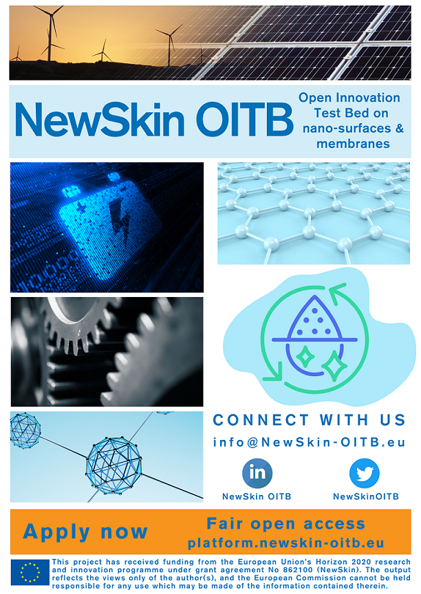
Graphene layers offer the potential for substantial advancements and enhanced efficiency in solar applications, energy storage, smart glass and even membranes (e. g. for seawater desalination) due to their remarkable properties, including transparency, barrier effects, and conductivity. Scalability issues have so far been a significant bottleneck in incorporating graphene into practical applications. Moreover, integrating graphene into current manufacturing processes presents a considerable technical challenge. NewSkin OITB partner Fraunhofer FEP have been working to improve this.
The absence of scalable deposition processes that maintain high layer quality at cost-effective throughputs has hindered the widespread adoption of graphene thus far. However, within NewSkin OITB, Fraunhofer FEP has devised innovative PECVD processes that facilitate the deposition of graphene at elevated process speeds, higher production throughput, and on a wider range of substrates at lower process temperatures. Thus overcoming scalability issues and integration challenges, that have so far been a bottleneck in the development and scaling of graphene deposition processes, and providing solid foundations for manufacturers in electronics and renewable energy sectors, to pursue further development and scaling of graphene coating processes.
Interested?