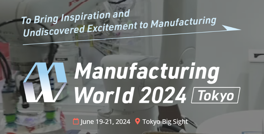
NewSkin OITB team at Manufacturing World Tokyo 19 - 21 June 2024 at booth No. E 53-11

NewSkin OITB team at Manufacturing World Tokyo 19 - 21 June 2024 at booth No. E 53-11
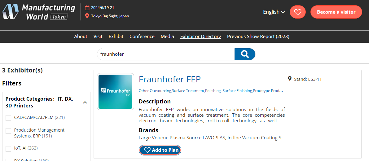
Published on 11 Jun 14:37 (about 2 years ago) by AquaTTDiscover the innovative PECVD processes and other competencies developed by NewSkin partner, Fraunhofer Institute for Electron Beam and Plasma Technology FEP, which allows for graphene deposition at high speeds, increased production throughputs, and use with a broader range of substrates at reduced temperatures!
Graphene layers hold the potential for significant advancements and improved efficiency in solar applications, energy storage, and smart glass applications, thanks to their exceptional properties such as transparency, barrier effect, and conductivity. The absence of scalable deposition processes that maintain high layer quality at cost-effective throughputs has hindered the widespread adoption of this promising material thus far. However, within the EU-funded project NewSkin (GA No. 862100), the Fraunhofer Institute for Electron Beam and Plasma Technology FEP has devised innovative PECVD processes that facilitate the deposition of graphene at elevated process speeds, higher production throughput, and on a wider range of substrates at lower process temperatures. Thus overcoming scalability issues and integration challenges, that have so far been a bottleneck in the development and scaling of graphene deposition processes, and providing solid foundations for manufacturers in electronics and renewable energy sectors, to pursue further development and scaling of graphene coating processes.
Interested? Join the team to discover & discuss more:
- Manufacturing World Tokyo, Japan
- June 19 - 21, 2024
- Booth No. E 53-11
>> Read more in Fraunhofer FEP press release here